Investigation into the effectivness of arrays of slots radiating through truncated waveguides to combat the formation of second order lobes
Watching second-order lobes collapse
A live polar radiation pattern of a six-element array. As the aperture excitation morphs from a uniform feed to a tapered (centre-weighted) distribution, the side-lobes fall away, the core mechanism this project uses to suppress second-order lobes.
Truncated slotted-waveguide array for second-order-lobe suppression
A single radiating slot was modelled in CST Studio Suite and characterised through a 23 × 21 parametric sweep of cavity-slot offset and length, 483 simulation cases. The extracted self-admittance seeded a spline-synthesised, non-uniform 6 × 6 truncated slotted-waveguide array of 36 elements. Against a −25 dB design target, the realised array reached a −23.2 dB side-lobe level at 9 GHz with a broadside main beam at ϕ = 90° and a 14.2° half-power beamwidth, comfortably past the −20 dB benchmark and 1.8 dB short of target, validating the approach as a preliminary optimisation method for truncated slotted waveguide arrays.
Single Slot Analysis
The single-slot analysis formed the electromagnetic foundation of the EGH490 research project. Before the final 6 × 6 truncated slotted waveguide array was implemented, a single cavity-backed radiating slot was isolated and studied in CST Studio Suite. This allowed the relationship between slot geometry, cavity offset, resonance, self-admittance, and radiating behaviour to be understood before array-level effects were introduced.
Why the Single Slot Was Studied First
The second-order lobe problem originates from the way energy is distributed across the radiating aperture. If the aperture excitation is poorly controlled, power is not concentrated into one clean main beam. Instead, part of the radiated energy is redirected into additional angular regions, producing unwanted sidelobes or second-order lobes.
For this reason, the project began with a single radiating slot rather than the full array. A single-slot model removes the complexity of mutual coupling between neighbouring elements and allows the behaviour of one aperture to be characterised in detail. The response of this individual slot then becomes the lookup basis for later slot-array synthesis.
Initial Single-Slot Waveguide Model
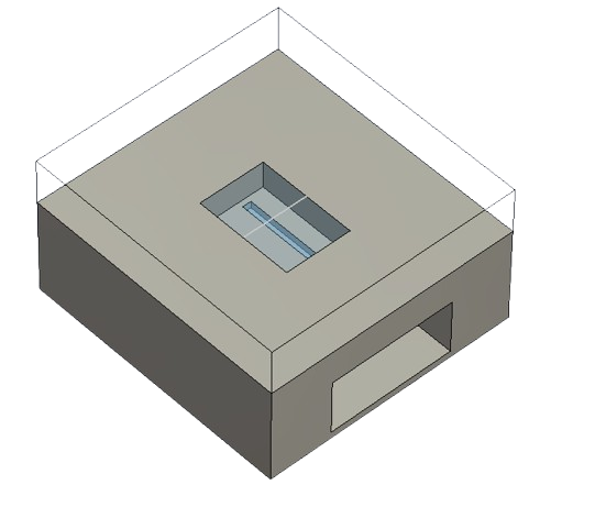
The single-slot geometry consisted of a rectangular waveguide section with a cavity-backed slot positioned on the upper surface. The model was simulated at 9 GHz in the X-band. The waveguide supported the dominant guided mode, while the slot and cavity region acted as a controlled discontinuity that allowed energy to couple out of the waveguide and radiate into free space.
The cavity-backed configuration was important because the cavity modifies the local field distribution around the aperture. Instead of treating the slot as a simple cut in a conducting wall, the project examined how the cavity length, slot offset, and slot geometry affected the strength and resonance of the radiating element.
Electromagnetic Design Parameters
The model was anchored to the X-band operating frequency of 9 GHz. Because the field propagates inside a rectangular waveguide, the dominant TE10 guided wavelength, not the free-space wavelength, set the longitudinal design reference, and the initial waveguide length was fixed to one guided wavelength.
| Operating frequency, f | 9.0 GHz (X-band) |
|---|---|
| Free-space wavelength, λ0 | 33.33 mm |
| TE10 guided wavelength, λ10 | 48.63 mm |
| Waveguide broad × narrow wall, a × b | 22.86 × 10.16 mm |
| Wall thickness, t | 1.27 mm |
| Wave impedance, Zwave | 550.0 Ω |
| Truncated cavity, L × W × D | 18 × 12 × 5 mm |
| Cavity slot, L × W × D | 16 × 1.588 × 1.27 mm |
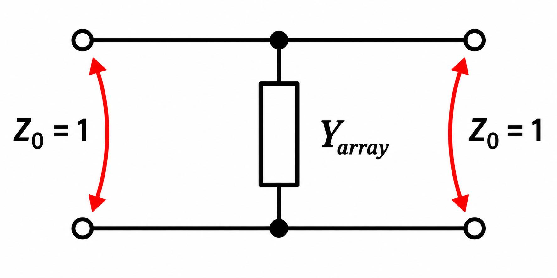
Equivalent Self-Admittance Model
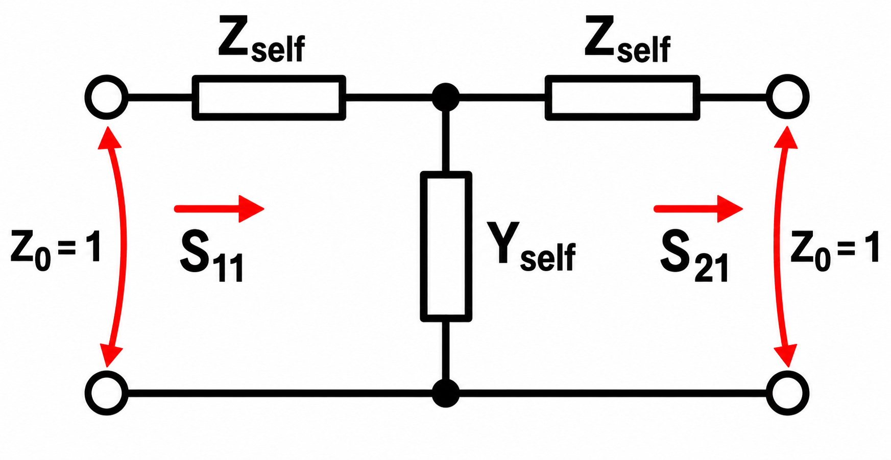
The single slot was interpreted using an equivalent two-port transmission-line representation. In this model, the waveguide ports define the input and output reference planes, while the radiating slot is represented as a shunt self-admittance placed across the transmission path.
The self-admittance is written as:
For the normalised two-port model (Z0 = 1), the complex self-admittance was extracted directly from the simulated scattering parameters:
The real component, Gself, represents the conductance associated with power coupled into the radiating aperture. A higher conductance generally indicates stronger radiation. The imaginary component, Bself, represents reactive stored energy around the aperture. When Bself approaches zero, the slot is near resonance.
This circuit model was used to translate CST scattering data into a form suitable for antenna-array synthesis. Instead of selecting slot dimensions by appearance alone, each geometry could be judged by its extracted conductance and susceptance.
Parametric Sweep Definition
A two-dimensional CST parametric sweep was conducted using the cavity-slot offset and cavity-slot length as the main design variables. The cavity-slot offset controlled the coupling strength between the guided mode and the aperture, while the cavity-slot length controlled the resonance condition.
For each geometry, the complex scattering parameters were exported and converted into self-admittance. This produced a database linking each pair of geometric parameters to its corresponding electromagnetic response.
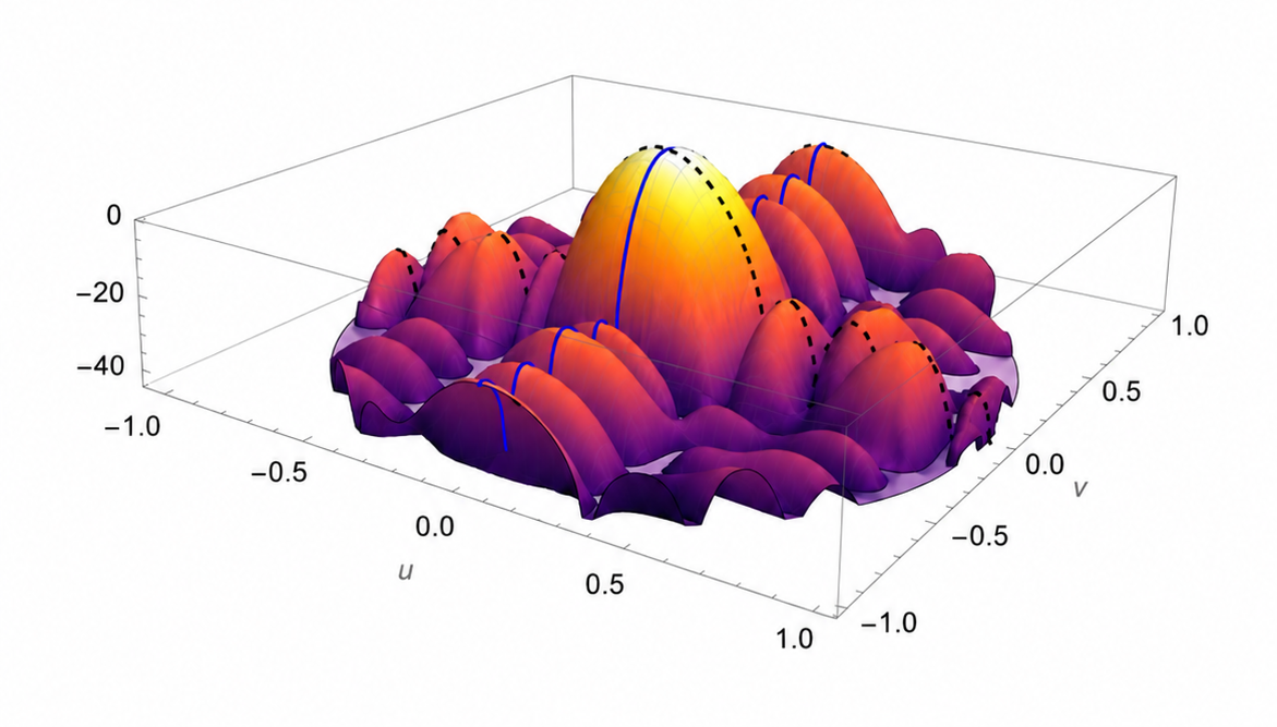
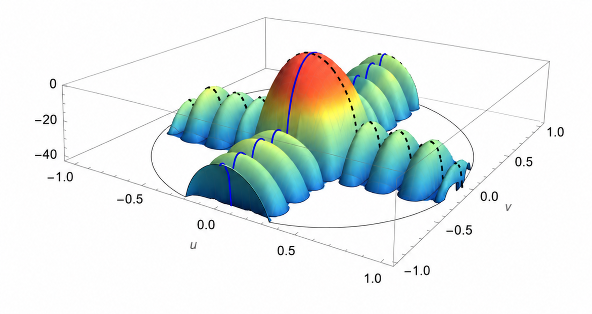
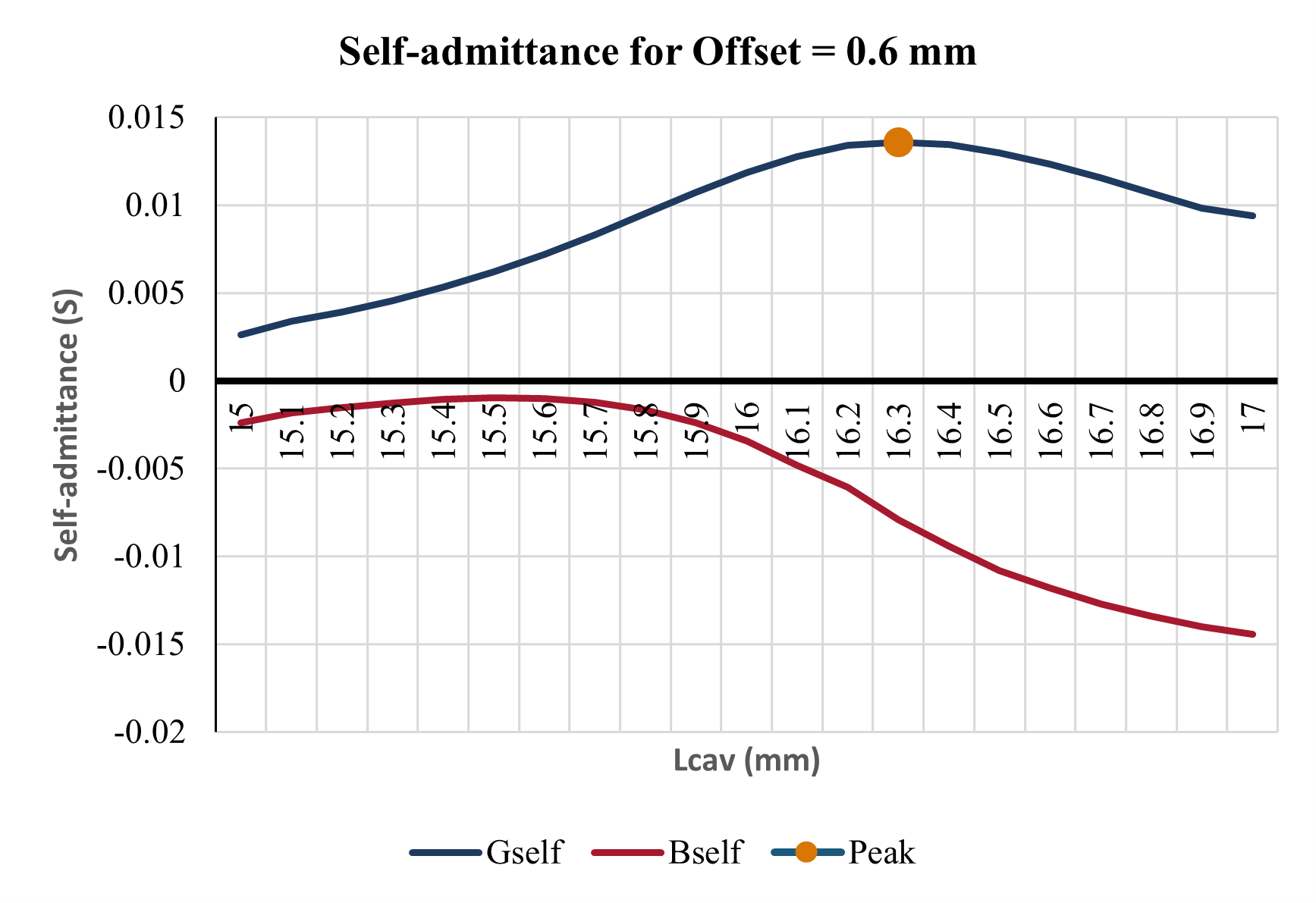
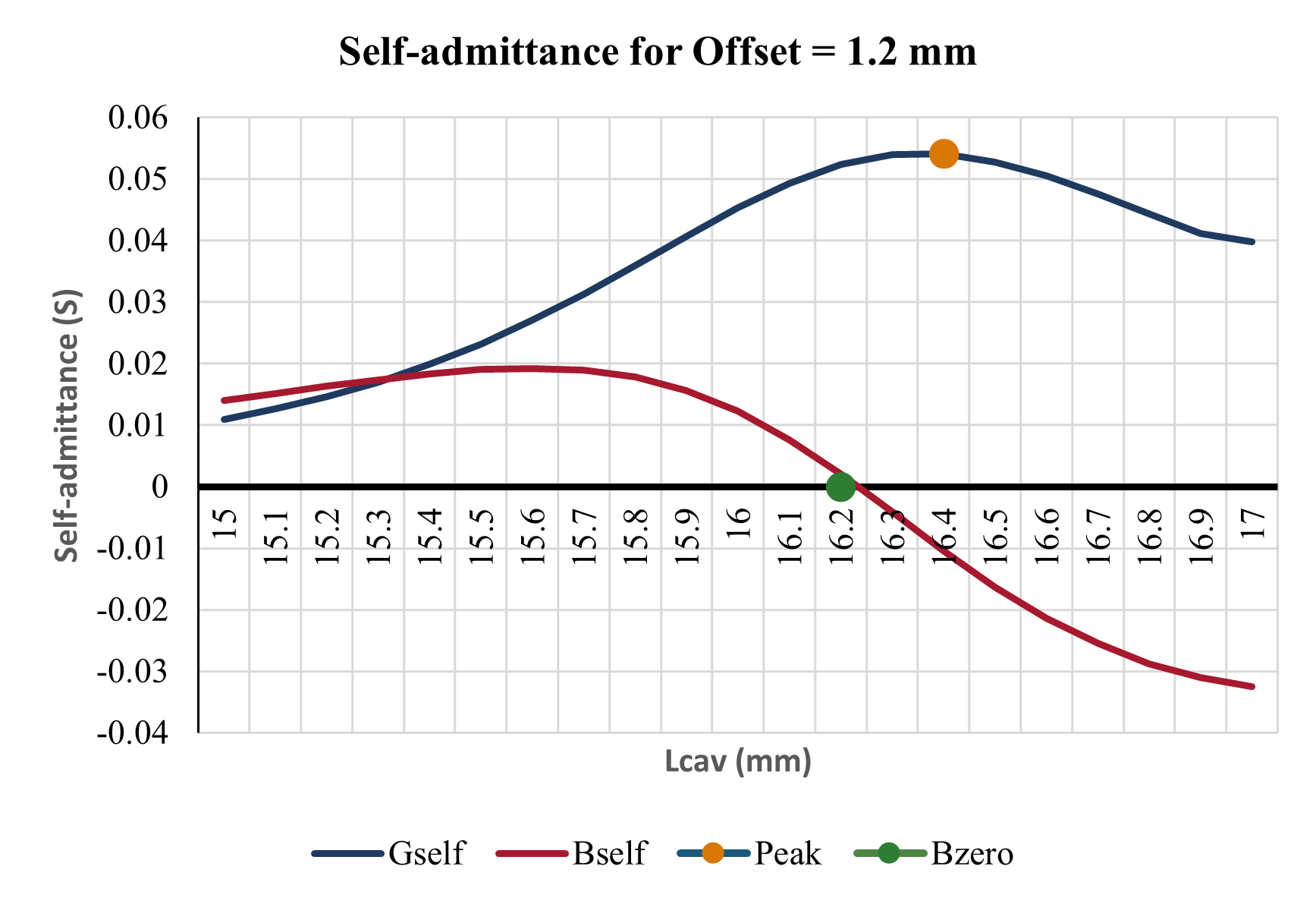
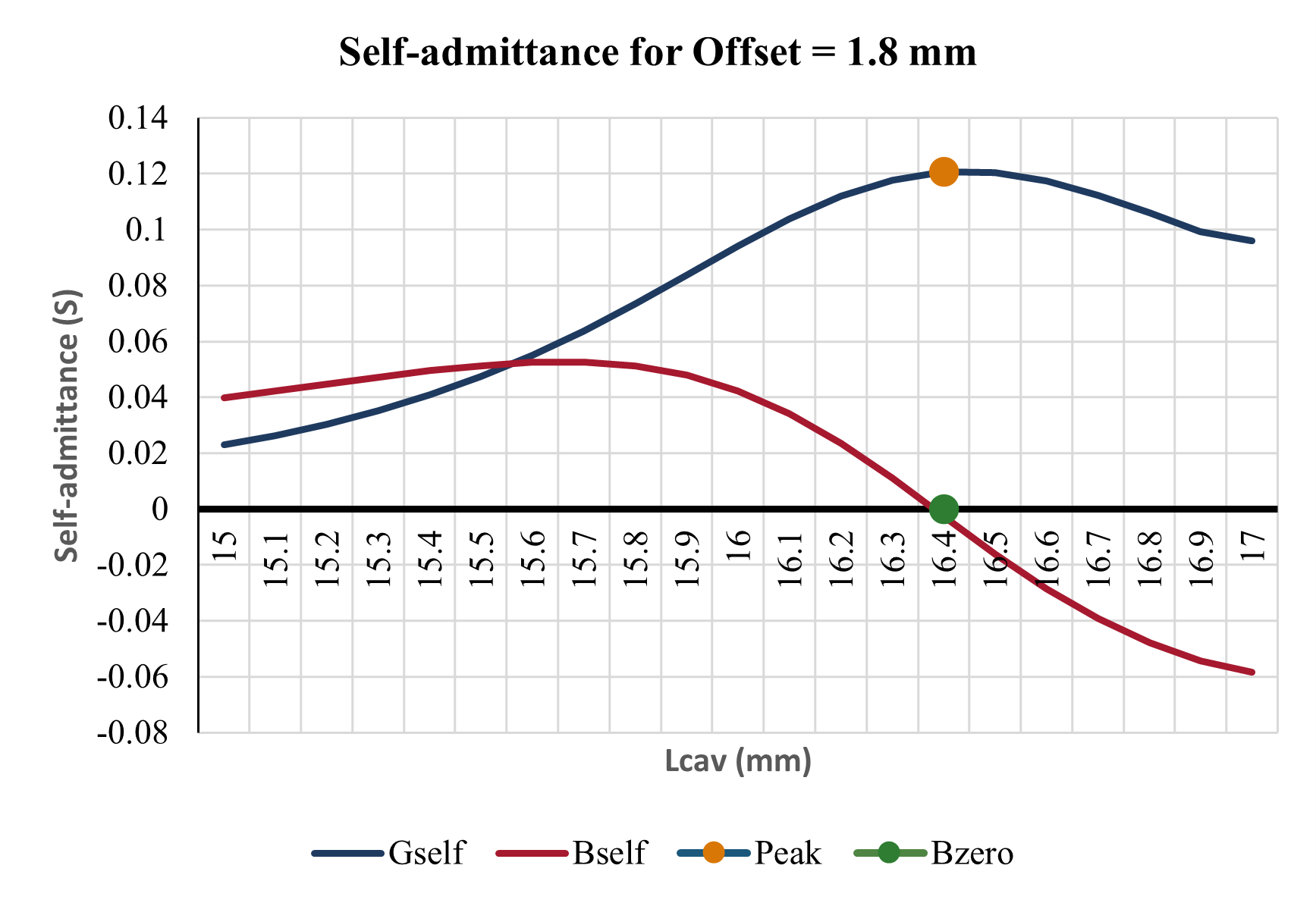
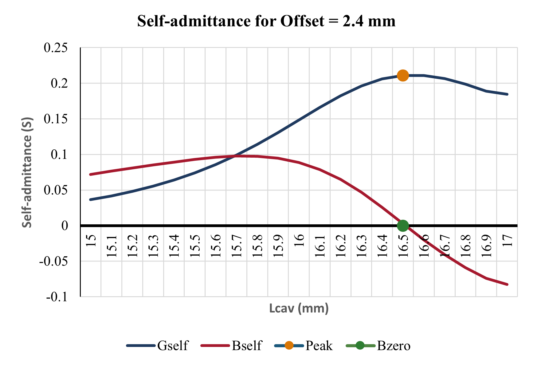
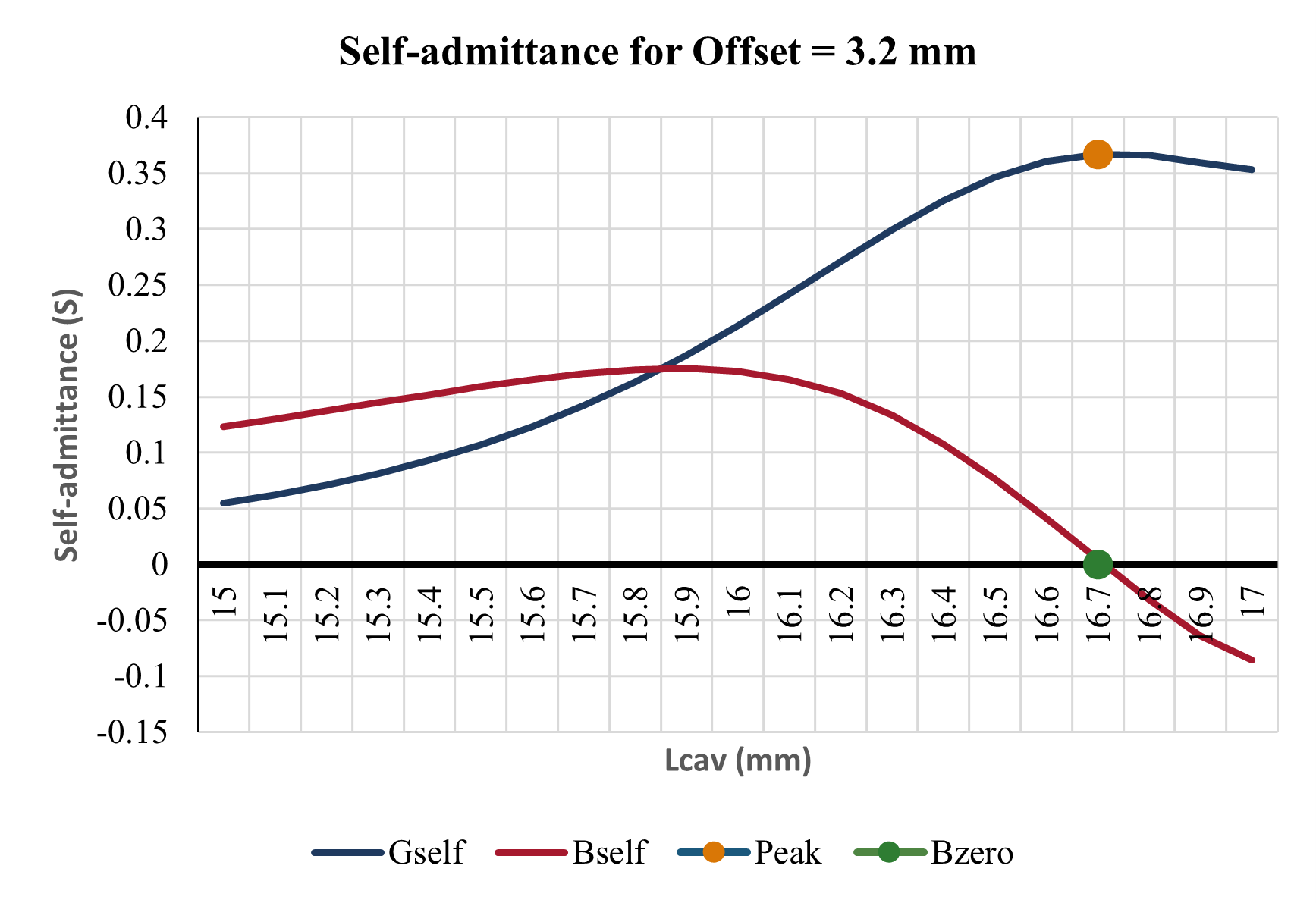
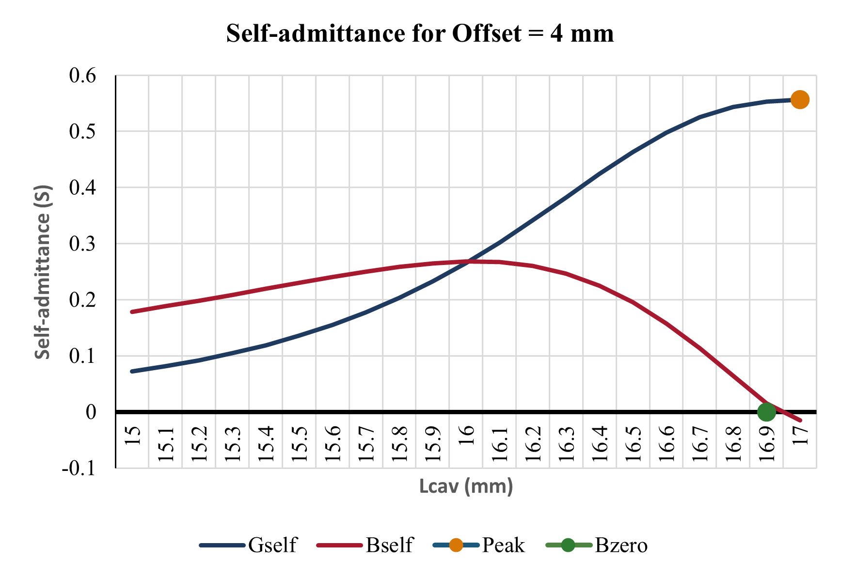
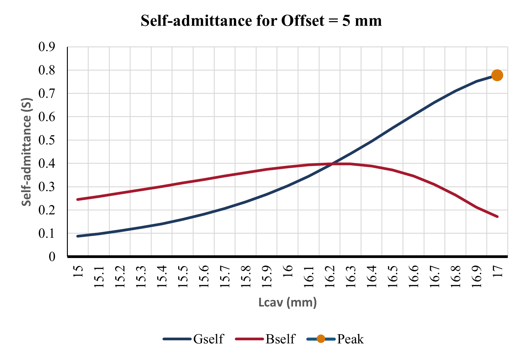
Self-Admittance Sweep Results
The representative sweep results show how the single-slot response changes as the cavity-slot offset is increased. At low offsets, the slot is weakly coupled and the self-conductance remains relatively small. As the offset increases, the peak conductance rises, indicating that more energy is coupled from the waveguide mode into the radiating aperture.
The design selection was not based on maximum conductance alone. A useful slot geometry must provide strong radiation while also remaining close to resonance. This occurs when Gself is high and Bself is close to zero.
Interpretation of the Sweep Results
The sweep results confirmed that slot offset has a strong influence on the radiating behaviour of the cavity-backed slot. Increasing the offset generally increases the peak value of Gself, showing that the slot couples more strongly to the guided wave as it is moved away from the centreline.
However, a high conductance value by itself does not guarantee a good design. If the susceptance remains large, the slot behaves as a strongly reactive discontinuity and may not operate efficiently at the intended frequency. The preferred region is therefore where conductance is locally high and susceptance is close to zero.
This single-slot database was then used as the design foundation for the full truncated 6 × 6 array. Through interpolation, each array element could be assigned its own cavity-slot offset and cavity-slot length. This allowed the final array to use a controlled non-uniform aperture rather than a repeated uniform slot pattern.
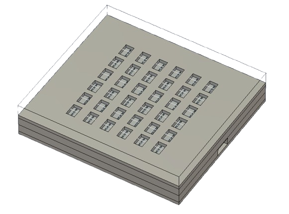
Multiarray Waveguide Design
After the single-slot self-admittance behaviour was characterised, the design was extended into a complete 6 × 6 truncated slotted waveguide array. This stage converted the isolated single-slot response into a full aperture structure, where the radiation pattern depends on the collective excitation, spacing, offset, and coupling behaviour of all 36 radiating elements.
Transition from Single Slot to Full Array
The full multiarray design was not created by repeating one identical slot geometry. Instead, the self-admittance data extracted from the single-slot CST sweep was used as a lookup basis for generating a non-uniform 6 × 6 slot distribution. Each slot was assigned its own cavity-slot offset and cavity-slot length so that the aperture excitation could be shaped deliberately.
This was a central design decision. A uniform slot array can produce strong repeated secondary lobes because each element contributes in a highly periodic way. By using non-uniform slot offsets and lengths, the aperture distribution can be tapered and controlled, reducing the strength of unwanted off-axis radiation while preserving the dominant main beam.
Array Equivalent-Circuit Interpretation
Once the complete 6 × 6 structure was assembled, the full array was interpreted using an equivalent shunt-admittance model. Unlike the single-slot case, the array admittance represents the combined electromagnetic loading of all radiating apertures, including radiation conductance, reactive aperture storage, cavity effects, and mutual coupling between neighbouring slots.
The conductance term represents real radiated power from the array, while the susceptance term represents stored reactive energy associated with the aperture and cavity fields. A useful array design must radiate effectively while remaining reasonably matched to the waveguide feed.
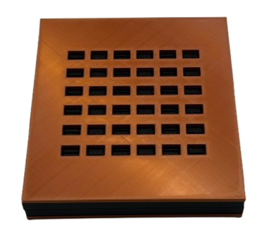
6 × 6 CST Geometry Implementation
The final CST model was implemented as a layered truncated-waveguide structure. The lower conductive layers defined the waveguide body and coupling path, while the upper layers introduced the radiating slots and cavity-backed aperture regions. The cavity features remained centred with respect to the waveguide, while the slot offsets varied according to the generated design table.
This layered construction allowed the model to preserve a consistent mechanical structure while using slot displacement as the primary mechanism for controlling local coupling strength. Because each slot contributes to the aperture field, small errors in slot placement, length, or layer alignment can alter the phase distribution and degrade the far-field response.
Far-Field Directivity and Lobe Suppression
The final far-field response was evaluated at 9 GHz using two principal angular cuts. The array produced a dominant broadside beam centred at 90 degrees. The sidelobe levels in both cuts were approximately −23.2 dB and −21.8 dB, which showed meaningful suppression but fell short of the −25 dB target.
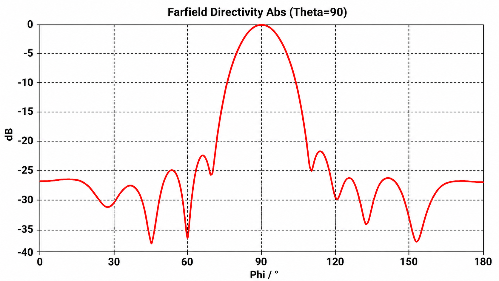
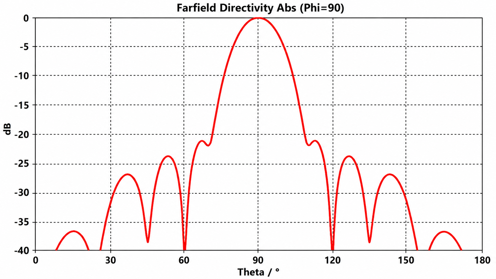
Both principal cuts placed the main lobe at ϕ = 90° (broadside), with a reported main-lobe magnitude of ≈ 0.143 dB. The constant-θ cut (θ = 90°) gave the stronger result; the constant-ϕ cut (ϕ = 90°) was marginally weaker. The input match minimum sat at ≈ −10.5 dB near 9.03 GHz, usable, though not deeply matched.
Smith Chart and Admittance Behaviour
The completed array was also assessed using Smith chart responses. The impedance and admittance views show that the array behaves as a frequency-dependent electromagnetic load. The match was usable but not fully optimised, indicating that the final geometry could radiate effectively while still leaving room for future refinement of the feed, slot offsets, cavity dimensions, or layer alignment.
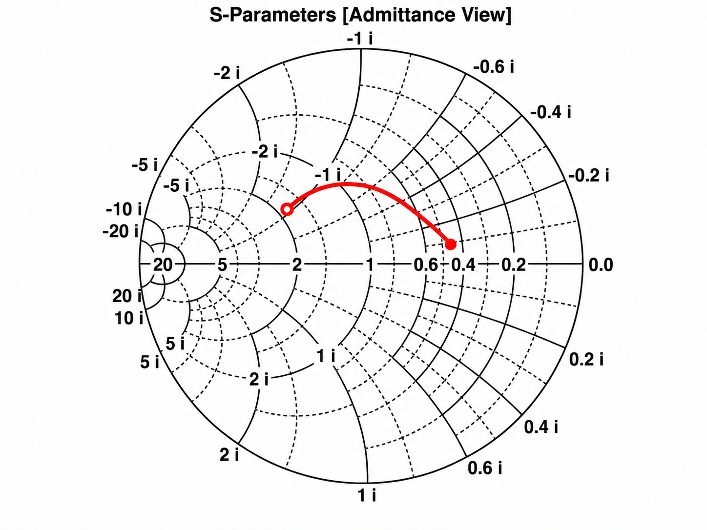
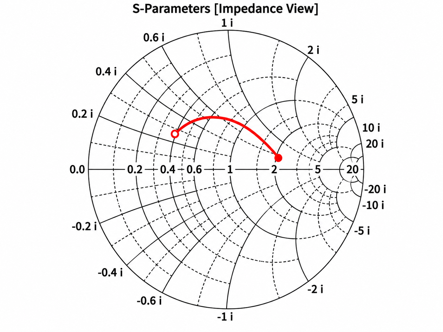
| Input impedance, Zin @ 8.9 GHz | ≈ 230 + j134 Ω |
|---|---|
| Input impedance, Zin @ 9.1 GHz | ≈ 1.14×10³ − j218 Ω |
| Input admittance, Yin @ 8.9 GHz | ≈ 3.25 − j1.89 mS |
| Input admittance, Yin @ 9.1 GHz | ≈ 0.85 + j0.16 mS |
Technical Interpretation
The multiarray results confirmed that the single-slot database could be extended into a practical array-level design. The final 6 × 6 layout produced a shaped aperture rather than a repeated uniform slot pattern. Stronger excitation was concentrated near the centre of the aperture, while weaker excitation occurred toward the edges. This tapering is important because it reduces abrupt aperture discontinuities and helps suppress secondary radiation maxima.
The CST simulation showed that the array produced a controlled broadside beam with sidelobes of approximately −23.2 dB and −21.8 dB in the principal planes. While this did not meet the project’s −25 dB target, it demonstrated that controlled cavity-slot offsets, cavity-slot lengths, and non-uniform aperture synthesis can reduce second-order lobe behaviour in a truncated slotted waveguide array.
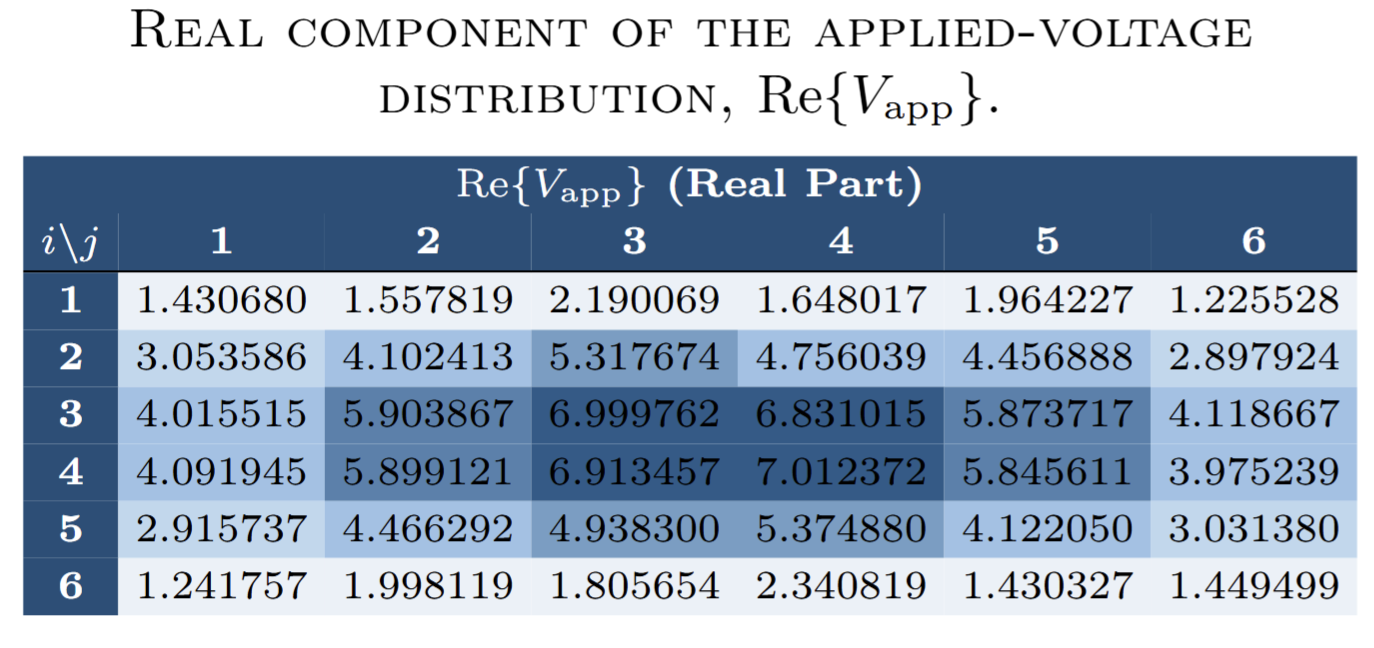
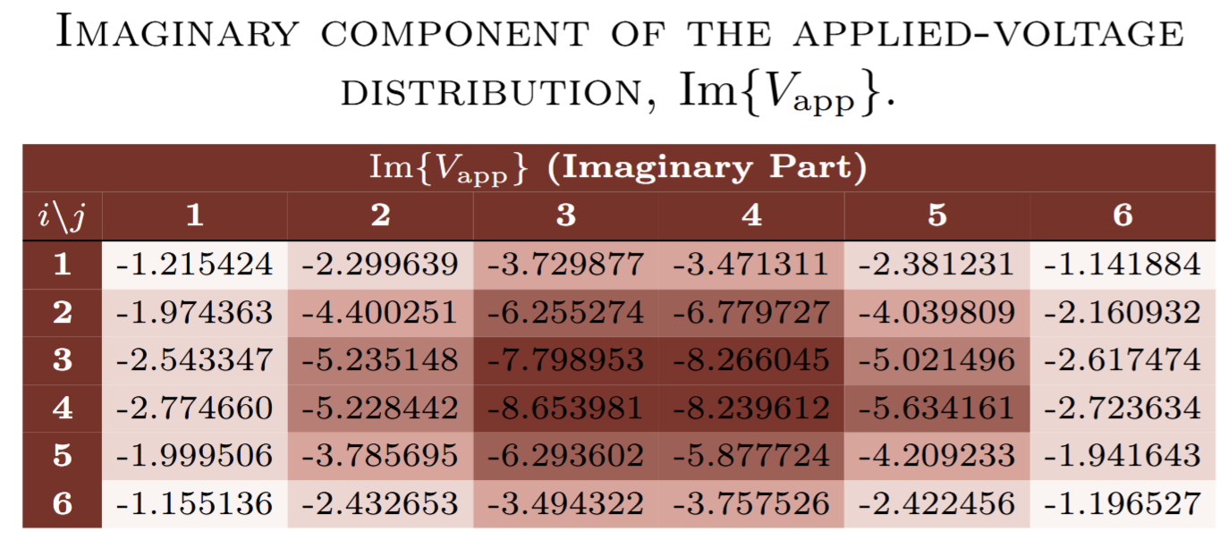
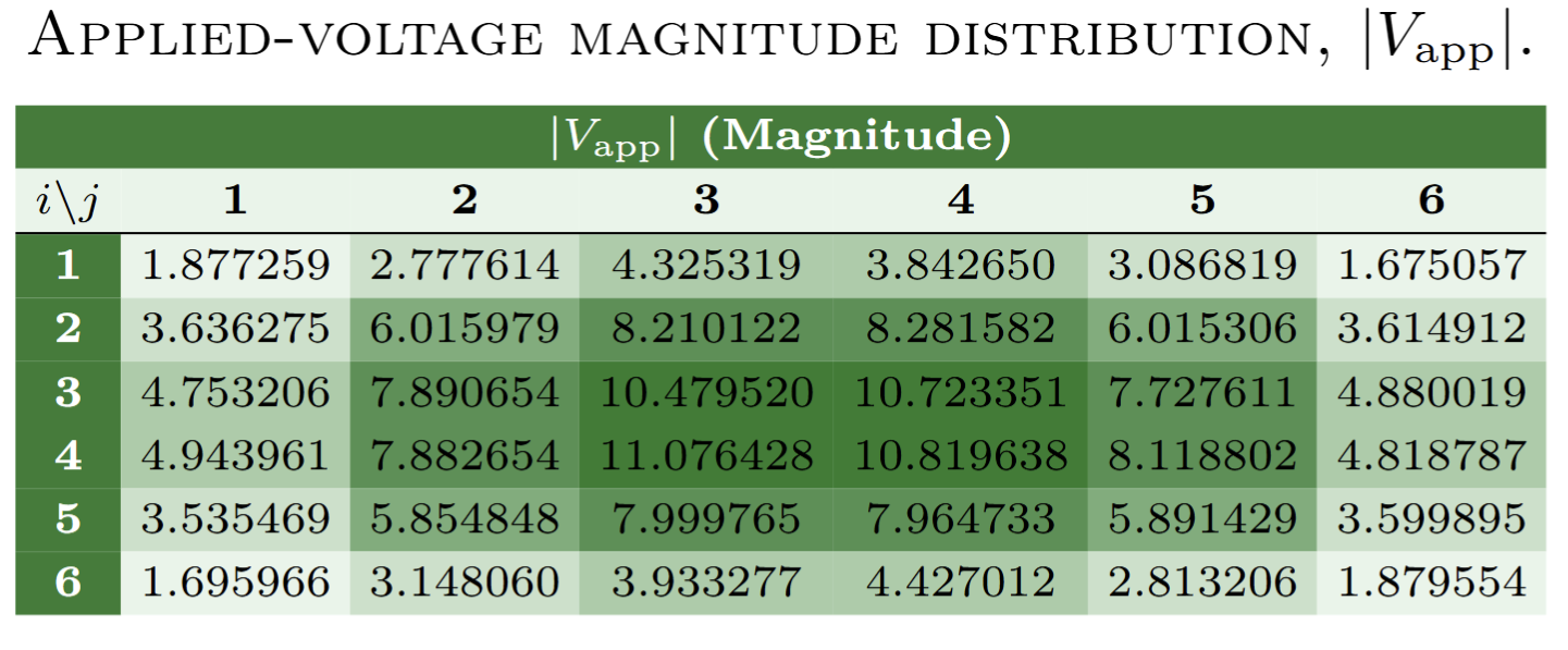
Applied-Voltage Matrix Analysis
The applied-voltage response of the final 6 × 6 slotted waveguide array was analysed to verify how the implemented cavity-slot and coupling-slot geometry shaped the aperture excitation. Since the applied voltage is complex, each element was separated into real and imaginary components before calculating the magnitude distribution across the array.
This analysis is important because the far-field radiation pattern is controlled by both the amplitude and phase of the aperture excitation. A clean main beam with reduced off-axis lobes requires the centre of the aperture to radiate more strongly than the edges, while avoiding excessive phase or magnitude irregularity between neighbouring elements.
Magnitude Distribution
The applied-voltage magnitude was calculated from the real and imaginary components. This magnitude represents the excitation strength of each slot element. Larger values indicate stronger local contribution to the radiating aperture, while lower values indicate weaker edge excitation.
The magnitude distribution confirms that the strongest excitation occurs around the central four elements of the 6 × 6 array. The outer elements, especially the corner elements, are much weaker. This produces a tapered aperture distribution, which is useful because it reduces abrupt edge discontinuities and helps suppress unwanted second-order lobes.
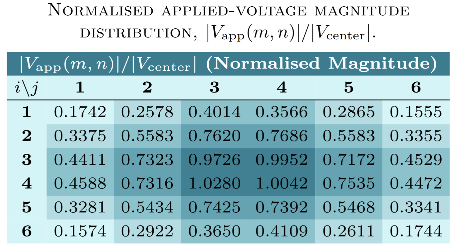
Normalised Aperture Excitation
Because the array has an even number of elements, there is no single physical centre element. The four central elements were therefore averaged to define the centre reference value. Every element magnitude was then normalised by this centre-four reference.
The normalised distribution shows that the centre elements remain close to unity, while the outer rows and columns reduce progressively toward the aperture edges. This confirms that the realised CST geometry produced the intended tapered excitation rather than a flat uniform aperture.
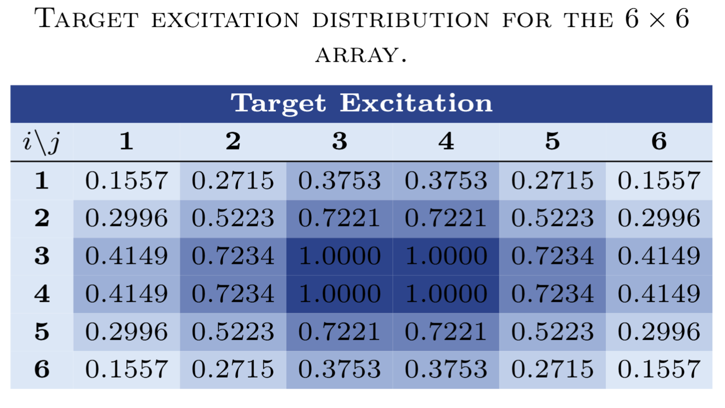
Comparison with Target Excitation
The target excitation matrix defined the desired aperture taper used to guide the array synthesis. It is symmetric about the centre of the 6 × 6 aperture, with the largest excitation assigned to the central four elements and progressively smaller values toward the outer rows and columns.
Comparing the realised normalised voltage distribution with this target matrix verified whether the implemented slot geometry reproduced the intended aperture weighting. The close agreement between the realised and target distributions supports the use of spline-generated cavity-slot offsets and lengths as a practical method for shaping the aperture response.
Applied-Voltage Verification Outcome
The applied-voltage matrices verified that the completed 6 × 6 geometry produced a centre-weighted aperture excitation. The central elements carried the strongest voltage response, while the edges and corners were reduced. This realised taper supports the suppression of second-order lobes by reducing abrupt aperture discontinuities and controlling the spatial distribution of radiated energy.
Outcome of the Multiarray Stage
The multiarray stage validated the transition from single-slot modelling to full-aperture antenna design. A complete 6 × 6 CST model was assembled, simulated, interpreted through equivalent admittance, verified using Smith charts, and evaluated through far-field directivity cuts. The final response showed meaningful suppression of unwanted second-order lobes while maintaining a dominant main beam.
Selected Bibliography
- C. A. Balanis, Antenna Theory: Analysis and Design, 4th ed. Hoboken, NJ: Wiley, 2016.
- J. L. Volakis (Ed.), Antenna Engineering Handbook, 4th ed. New York: McGraw-Hill, 2007.
- L. Josefsson and S. R. Rengarajan, Slotted Waveguide Array Antennas: Theory, Analysis and Design. London: IET, 2018.
- H. M. El Misilmani, M. Al-Husseini, and K. Y. Kabalan, “Design of slotted waveguide antennas with low sidelobes for high power microwave applications,” Progress In Electromagnetics Research C, vol. 56, pp. 15–28, 2015.
- P. Delos, B. Broughton, and J. Kraft, “Phased array antenna patterns, Part 2: Grating lobes and beam squint,” Analog Devices Analog Dialogue, 2020.
- Y.-S. Yeoh and K.-S. Min, “Characteristics of 6 × 26 slotted waveguide array antenna for wave monitoring radar,” J. Electromagn. Eng. Sci., vol. 21, no. 5, pp. 439–447, 2021.
- B. M. Yousef et al., “Ultra-low SLL slotted waveguide antenna array using groove-gap waveguide technology for millimeter-wave applications,” AEU – Int. J. Electron. Commun., 2024.
EGH490 Honours Research Project · Bachelor of Engineering (Electrical & Aerospace) · Queensland University of Technology · Supervised by Dr Jacob Coetzee · May 2026.